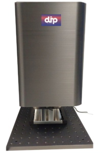
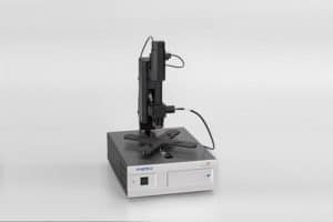
Optical profilometer D-Surface-View D-surface-View 1. Local and global inspection from mm to nm 2. Measurement in a single acquisition 3. Nanoscale D-Surface View is intended to help manufacturers of wafers up to 300mm in diameter reduce costs and for chipmakers to improve yields of devices manufactured with best-in-class process technology. The equipment can be used […]
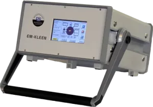
Remote plasma cleaner Semi-Kleen &EM- Kleen Series Plasma cleaning solution for contamination control in high vacuum systems, such as SEM, FIB, AES, XPS, ALD, EUVL, etc. SEMI-KLEEN and EM-KLEEN series remote plasma cleaners were based on the high efficiency inductively coupled plasma (ICP) discharge technology developed at the Lawrence Berkeley National Laboratory. Our patent pending […]
Plasma Cleaners Tergeo series Tergeo series tabletop plasma cleaners 1. Intelligent and intuitive design 2. Quantitative plasma measurement technology3. Immersion and downstream plasma processing modes in one system4. Recipe and job sequence5. Pulsed operation Why choose Tergeo plasma cleaner Better plasma uniformity with external electrode design Unique plasma sensor technology for quantitative plasma strength measurement […]
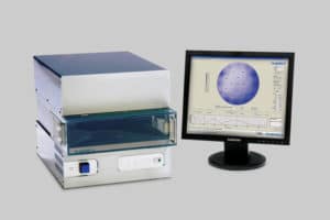
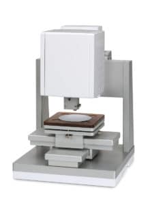
Automated thin-film thickness mapping F60 1. Dedicated to production 2. Automated 3. Fast 4. Customizable The F60-t family maps film thickness and index just like our F50 products, but it also includes a number of features intended specifically for production environments. These include automatic notch finding, automatic on-board baselining, an enclosed measurement stage with motion interlock, […]
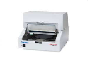
Automated thin-film thickness mapping F54- XY-200 1. Sample up to 200mm in diameter 2. Automated XY stage 3. Thin, thick, rough and opaque films Thin-film thickness on samples up to 200mm by 200mm is easily mapped with the F54-XY-200 advanced spectral reflectance system. The motorized X-Y stage moves automatically to specified measurement locations, facilitating thickness […]
Automated thin-film thickness mapping F54 1. Sample up to 450 mm in diameter 2. No limit on the number of points 3. Easy to use 4. Wide wavelength range Thin-film thickness of samples up to 450 mm in diameter are mapped quickly and easily with the F54 advanced spectral reflectance system. The motorized r-theta stage moves automatically […]
Spot measurement – High thickness F70 1. Built-in online diagnostics 2. Standalone software included 3. Sophisticated history function for saving, reproducing, and plotting results The F70s are general-purpose thickness measurement instruments that are capable of measuring thicknesses up to 15mm. Common applications include glass and plastic sheets, lenses, and containers and semiconductor wafers. The basic […]
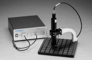
Resistivity & conductivity mapping R50 Serie 1. Four-point probe and eddy-current probe systems 2. Sample mapping in rectangular, linear, polar and custom configurations 3. X-Y travel up to 200mm 4. Measure a ten-decade range of sheet resistance on conductive and semi-conductive films 5. Contact and non-contact measurement Filmetrics® sheet resistance measurement tools marry the technology […]
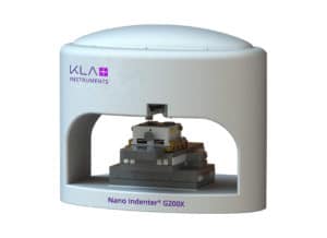
Precision Nanoindenter G200X 1. Easy to use and user-friendly 2. Mechanical test at the nanometric scale 3. Precise quantitative results 4. Large variety of sample The Nano Indenter G200X provides an easy-to-use nanoscale mechanical tester that quickly delivers accurate, quantitative results. The G200X system handles a wide variety of samples from hard coatings to soft […]
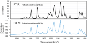
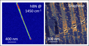
Photo-induced Force Microscopy (PiFM) Nano-IR PiFM Technology 1. Best of Nano-IR and Scanning Near-Field Optical Microscopy 2. Exceptional Spatial Resolution in Chemical Mapping 3. Excellent Sensitivity 4. Good Correlation between PiFM and Conventional IR Spectra 5. Universal Sample Applicability 6. Hyperspectral Nano-IR Imaging PiFM – Best of Nano-IR and Scanning Near-Field Optical Microscopy Nano-IR (nanoscale infrared […]
AFM IR microscope Vista-IR 1. Robust and easy nanoscale chemical imaging and spectroscopy 2. Nanoscale chemical mapping of inorganics and biomolecules based on their IR vibrational modes 3. High surface sensitive technique 4. Works with both Transparentand Opaque substrates 5. Non-contact and Tapping Method 6. Standard off-the-shelf cantilever 7. Works in visible and mid-IR spectrum […]
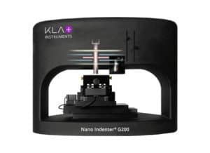
Nanoindenter at nanoscale G200 1. Accurate, flexible and user-friendly 2. Mechanical test at the nanometric scale 3. Scalable and extensible platform 4. Automated The G200 Nanoindenteur system is a precise, flexible and user-friendly instrument for mechanical testing at the nanometric scale. It is a fully scalable, scalable, production-proven platform with automated high-throughput hardness measurement […]


